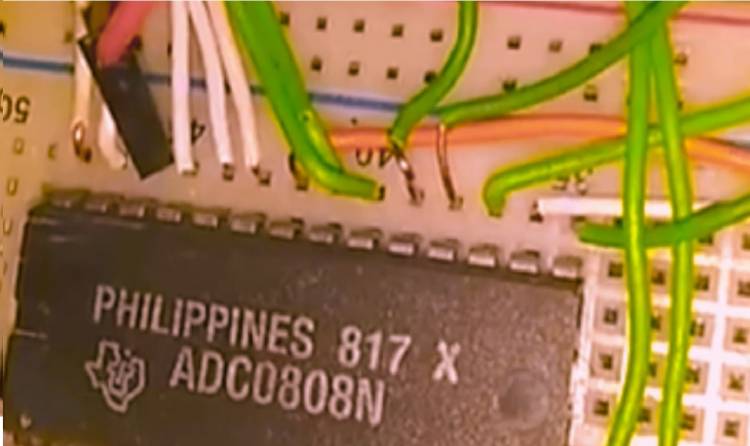
Analog Digital Converter ADC00808
Analogue signal processing is an important topic. The conversion of analog signals to digital signals has become very important, especially today. One of the most important issues when processing analog signal is multi-channel analog signal processing. Here, ADC0808 provides us with the opportunity to process many signals simultaneously with 8 analog input channels.
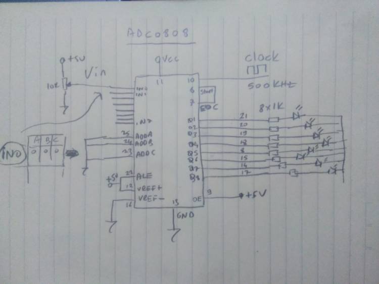
Let's examine the technical specifications of the ADC0808:
It has a cycle time of 100 microseconds. This period is valid for a single channel. 800 microseconds is used for 8 analog channels.
8 ADDA, ADDB, ADDC pins are used to select analog input pins. These pins can be "1" or "0". When they are all “1”, it is 8 in the decimal plane and the IN7 analog input of the ADC0808 is selected. When ADDA, ADDB, ADDC pins are “0”, “0”, “0” respectively, analog input IN0 is selected. As can be seen from the examples, when we make inputs in binary number system between “0”, “0”, “0” and “1”, “1”, “1” to ADDA, ADDB, ADDC pins, we can select analog input pins from IN0 to IN7.
The ADC0808 has an external clock input. The frequency of the square wave signal we apply to this pin can be up to 1280 KHz.
The OE pin must be at the "1" level in order to see the digital signal at the output.
ALE: When set to “1”, analog signal channel selector ADDA, ADDB, ADDC information is written to “LATCH”. It becomes clear from which channel the analog signal will be accepted.
START pin: When it goes from “0” to “1”, signal cycle starts.
The circuit we are implementing is an independent circuit. In systems with microprocessor or microcontroller, using RD, WR, IO control, Address pins of microprocessor and microcontroller chips, ADC0808's selection pins can be activated or passive, and analogue signal reading can be made in a controlled manner.
On our Youtube channel, you can review the video of the application we have made before.